
How does an RF circuit board interact with antennas?
RF circuit board interact with antennas
An RF circuit board interacts with antennas in a variety of ways. Its materials, layout, and grounding all contribute to signal transmission and power dissipation. In addition, its conductive paths must be designed to minimize impedance mismatches and signal reflections that can degrade signal quality. This is especially important when an RF circuit board must operate at high frequencies or in a congested environment.
An rf circuit board needs to be made from special laminates that can withstand high temperatures and frequencies and that have the right dielectric constant and loss tangent angle. Typical materials used in PCB manufacturing, such as FR-4, have a poor dielectric constant and low loss tangent angle, which makes them unsuitable for RF PCBs. Specialized PCB materials with a dielectric constant and loss tangent angle better suited to RF applications include FEP, PTFE, ceramics, hydrocarbons, and different forms of glass.
The RF section of the PCB should be separated from other sections to avoid causing interference and introducing noise. This can be accomplished by designing the RF layer as a no-go zone for digital signals, which should only be routed through the inner layers. The RF layer should also be properly decoupled from the chip’s power supply. If it isn’t, high-power amplifiers can generate significant noise and cause self-oscillation.
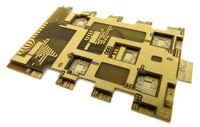
How does an RF circuit board interact with antennas?
For RF signals, the signal path should be as short as possible to reduce insertion loss and electromagnetic interference. It should also be routed away from high-speed digital traces, power planes, and other sources of noise. Impedance matching is crucial for RF circuits to ensure that the source and load characteristic impedances match. Impedance mismatching can result in signal reflections that cause loss of power and distortion of the signal waveform.
In addition, the design of an RF PCB should include a solid ground plane to reduce signal losses due to parasitic inductance. Via size is also a factor. Ideally, via diameter should be no larger than 1/20th of the signal wavelength. Additionally, buried vias should be avoided, as they increase parasitic inductance. Instead, use stitching to connect the top and inner ground planes of an RF circuit board. This helps to create shorter return paths and improves the grounding of traces and signal radiated from the RF section.
RF signals require a good grounding for proper operation. The grounding must be large enough to eliminate the effects of radiated and conducted noise. It must also be well decoupled from the power supply of the RF chips to prevent interference and induced currents that can lead to instability or even self-oscillation.
The grounding of an RF circuit board can be achieved by using a combination of via stitching, copper bridges, and metal shielding to create a continuous grounding network. The pattern of the grounding should be as regular as possible to avoid isolated areas that can act as unintended antennas and create ground loops. Lastly, it’s essential to maintain adequate clearance between the RF traces and the ground pours to ensure manufacturability and prevent solder bridges during assembly.